 MIMIC (MetricMind Infrared-Modulated Intelligent Clamper)
Copyright© 2009 Metric Mind Corporation
MIMIC (MetricMind Infrared-Modulated Intelligent Clamper)
Copyright© 2009 Metric Mind Corporation
Simple analog BMS for tinkering man – part I
By Victor Tikhonov
President/CTO
Metric Mind Corporation
Published Nov. 11 2012.
I honestly don’t think there is any rationally thinking fellow out there who believes an EV battery battery pack composed from modern lithium cells does not need a management system which is suppose to make sure the pack and individual cells work within allowed limits. No one would dare to just wire cells together and forget it, cycling whole pack as one single cell.
However, to answer question if one needs some kind of a physical BMS installed in the vehicle, the answer is certainly no. There are two ways to deal with this issue. Battery management can be carried out by hardware doing the work for you, or by YOU, the battery manager, if you don’t mind doing necessary work yourself. But it must be one or the other. Most people will use some sort of BMS to automate this tedious task and take care of the battery consistently 24/7/365 without getting tired, distracted, calling sick or procrastinating until weekend. But since such convenience of a BMS obviously comes at cost, some people decide they’d rather manage their battery manually. Either way works well provided you know what you’re doing. (There is third group of people who believe and advocate no lithium battery or cells supervision needed at all, as if battery pack is magically selfcuring, but we’re not going to debate this or invalidate their ideas here. That’s what natural section is for).
Thinking how to simplify battery supervision system, in around 2004 I came up with minimalist cell clamper design. This was simply amplified classic shunt regulator built around TL-431 adjustable shunt. 96 clampers were installed in my ACRX – second reincarnation of Honda CRX conversion with AC drive done in 1995 (still in service today). It worked well with good cells but could not cope with Thunder-Sky’s inferior cells supplied to a group of 11 first adopters of then new Lithium battery group buy. Those who were into EVs 10 years ago when no one was running on lithium yet, might remember the story. Anyway, this clamper design for TS cells was predecessor of what became known as MIMIC (MetricMind Infrared-Modulated Intelligent Clamper). This design was contributed to the Tumanako project initiated by Green Stage company (New Zealand) and then released to public domain. Guys running this project not only listed this design along its sub-projects, but also helped me to write initial software for it to get started. Today I wanted to share a flavor of MIMIC I re-designed with my fellow EV’ers in mind, for whom simplicity, affordability and ability to make it themselves from plans often outweigh sophistication and completeness of more advanced OEM-like BMS systems. While, as name implies, original design used infrared light for data transmission (and baby PICs to process data), the version described here is modified in 2 major ways, which makes it reproducible by anyone with basic skills in assembling electronic circuits:
With wide acceptance of lithium batteries many BMS designs came out in recent years. While varying in complexity, majority of them share common passive balancing concept. In essence such BMS consists of remote voltage (and usually temperature) measurement system and array of remotely controlled shunt resistors, one across each cell. Normally it also takes care of auxiliary functions such as controlling main contactors and charger. It works like this: after cells voltage, temperature and sometimes capacity data is collected and massaged, based on some proprietary algorithm decision is made which cells to shunt and when. This is usually done during charging so the overall capacity of the pack is not reduced due to balancing activity. When a cell on charge is shunted, current that used to flow entirely through it is split in two paths thus reducing cell’s share of total current. This causes shunted cell be charged at slower rate, thus accumulate less Ah over time then un-shunted cells do. Since with passive balancing charge can only be removed, only cells with "extra" charge are shunted. The goal is to keep all cells in balance at all times. Sounds simple, but first difficulty comes from ambiguity of definition “cell balance”.
The term “balance” applies to cell SOC, not cell voltage. A pack is considered balanced when all its cells are at equal SOC. Some BMS systems declare pack balanced when each cell contains the same amount of Ah at all times instead of having the same SOC. Many proprietary OEM systems use at least both (and often – more) criteria, like internal impedance to determine SOC balance condition.
However, home made amateur BMS systems, often substitute cell SOC for cell voltage, and declare whole pack balanced simply when cells voltages are equalized. Anybody (well, almost) can measure voltage remotely. This method, however, may or may not present problem depending on whether cell’s voltage really represents its SOC for given flavor of lithium chemistry. Voltage based balance works well, for instance, for LiPo cells, but won’t work very well for lately popular LiFePO4 cells. Why? Problem is, voltage across each LiFePO4 cell does not change throughout most of its working region (between ~15…20% SOC and ~80…85% SOC), so meaningful voltage measurements can be done only outside this region – exactly where you don’t want the cells to be. Moreover, at low temperatures terminal voltage of a cell will actually rise while cell being discharged! (This happens because falling internal resistance as sell gets warmer rises terminal voltage at faster rate than decreasing SOC lowers it). This will certainly confuse voltage based balancing BMS unless smart compensation based on a lot of empirical data or good modeling is deployed. Other parameters such as charge/discharge rate, cycle life, calendar life and even cell shape (pouch, cylindrical or prismatic) affects voltage/SOC relationship in a ways even manufacturer often has no data about.
If voltage balancing starts only when SOC reach 80-85% (some people prefer to “bottom balance e.g. while cells are discharged, in this case when SOC reach 15…20%) where voltage finally begins more-less represent SOC, it’s too late – there is no enough time to balance voltages before pack is full (or empty) - that is, unless you use monstrous force cooled multi-amp shunts – a sign of crude BMS whose aggressiveness either substitute for intelligence of more sophisticated predictive balance strategies, or meant to deal with substandard cells whose parameters are all over the map. This is because the time during which you could gradually take out necessary amount of Ah out of cells with low shunt current over relatively long course of bulk charging is lost. However, again, accurate SOC tracking, impedance measurement and interpretation, and predictive modeling of cell behavior is far more difficult to implement than just remotely measuring voltages. Therefore for simplicity (read - cheaper, quick-to-market implementations), voltage balancing is being done over and over – it often outweighs ineffectiveness of whole system.
Remember, no two cells are identical. And a BMS is there not to fix bad cells, it won't and it can’t. Add to this the fact that amateurs don’t have luxury to cherry pick and match cells for their packs and [unlike for OEM packs] their cells might come from different manufacturing batches. Interaction of all these parameters makes accurate estimation of SOC based on just cell voltage measurement alone impossible, no matter how accurate readout is.
The subject of this article, however, is not to debate whether equalizing voltages instead of SOC is good or even valid idea or to criticize designs of such BMS’es. For many one-off battery systems this can be acceptable compromise, and if done right it will work well enough. Especially because in amateur EV projects, where most people love tinkering with hardware and periodically will intervene and manually take care of measuring and rebalancing, thus compensating for lacking system intelligence. If you happen to be one of those people, this article is for you. It just describes one possible hardware implementation of such BMS’ing method without endorsing it.
For a fixed clamper circuit in its simplest form, it would be enough to have something like a powerful Zener diode or its equivalent across each cell. It will start bypassing fraction of charging current after certain voltage threshold is reached. The main problems with this approach are:
Substituting single Zener diode by few forward biased SiC Schottky diodes greatly diminishes temp. dependence and power dissipation per device, and is absolutely simplest and cheapest practical clamp circuit I could come up with. You can also make Zener equivalent (transistor amplifier with or without help of an OpAmp) so it becomes adjustable, or use window comparators (as was done in my Smooth Talk hardware based BMS), but the main issue with any such clamper remains the same: constant breakdown voltage cannot track cell voltage or get adjusted remotely. Therefore a fixed clamper can only protect cell from overcharge when its voltage hits certain threshold. Below this point), clampers are useless – if cells are cycled in the middle of charge/discharge curve, such clampers simply never get chance to clamp. MIMIC addresses these issues as following:
As with any passive balance BMS’es, the power is dissipated on bypass power resistor. And as with any crude voltage measurement based BMS, it starts working well only when cell voltages deviate from average far enough, e.g. for LiFePO4 chemistry - near the end of charge. It works much better with LiPo cells, original LiIon cells or any chemistry where voltage more-less represents SOC. The relationship doesn’t have to be linear as with lead acid batteries, it just has to be monotonic.
The core of MIMIC module is unambiguous 555 timer and the highest cost component is power resistor. This makes MIMIC very inexpensive – about just $5…$7 worth of electronic components per cell, and entire system for high voltage pack can probably be built for well under $500.
Please note that MIMIC is not a substitute for a real BMS. It has no memory, no stored algorithms or battery models. It does not control charger or main contactors. It is pure analog hardware solution for what the name implies – intelligent clamper. It does not know what the voltage of each cell is. All it knows at any time if a cell voltage exceeds average, and if so, acts upon it. MIMIC shunts higher than average cells with variable rate proportional to the degree of discrepancy. MIMIC will ignore cells with voltages lower than running average. However, there are means to visually check for any low cells in the pack. Finally, there are no fancy displays for each cell, but I don’t think this is necessary. (Think of Nissan Leaf – thousands of their drivers not only have no per cell display, but even have no idea how many cells their battery has. Yet, they drive every day just fine with only "OK"/"Not OK" idiot light as long as they are confident the battery is taken care of by its electronics).
My background is hardware design (mostly – analog), but I’m no programmer. So I designed MIMIC with I believe one important feature - anyone who have sufficient basic knowledge about assembling electronic circuits can build it. The system might require troubleshooting, but never debugging. It is like old fashion transistor radio – if assembled from known good components with no mistakes, it is pretty much guaranteed to work.
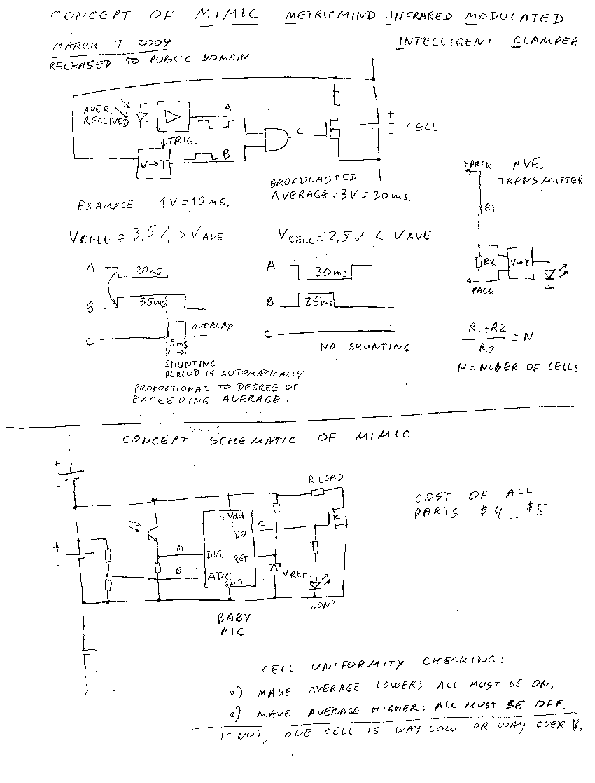
So, how does it work? The concept is very simple and depicted on fig. 1.
Incoming inverted pulse A (delivered to each MIMIC module from common transmitter) whose length t3-t1 is proportional to average (“ideal”) cell voltage is logically AND’ed with locally generated by each MIMIC module pulse B, whose length is proportional to the voltage of cell being monitored. The output of AND operation (pulse C) directly drives FET switch connecting shunting resistor across the cell. That’s really all there is to it!
There are two distinct conditions – when cell voltage is less then (or equal to) average, and when it is greater. First condition depicted on top of fig 1. B=t2-t1 is shorter than A=t3-t1. Therefore there are no positive overlaps of both pulses, so A*B=C remains zero and no shunting occur.
Another condition is when measured voltage exceeds average reference as shown at the bottom of fig. 2. In this case B=t4-t1 becomes longer than A=t3-t1. Logic AND of both pulses yields overlapping pulse C=t4-t3 whose length is the difference between B and A, and that is proportional to the voltage difference between monitored cell and ideal average cell. The more the difference – the longer pulse C is, thus longer shunting time. So, more Ah taken out of the cell one pulse at the time, until cell’s voltage becomes equal to the average.
Because transmitted average cell voltage (e.g. A length) changes as whole pack is charged or discharged, it is precisely being tracked by every MIMIC – each cell gets compared to ideal average one. Think of all MIMICs as means to make sure total pack voltage is divided among all cells exactly equally, and if it isn’t – they ill correct for it.
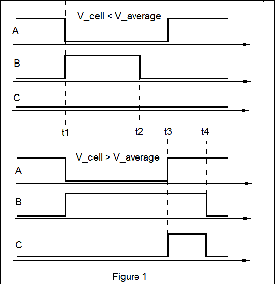
An electrical schematic of a single MIMIC module installed on each cell is presented on fig. 2. How does it work?
Fig. 2. MIMIC module.
The heart of the circuit is voltage to time period converter built around U1 timer chip. I arranged circuit in a bit unconventional manner to turn it into a Vdd supply voltage to time period converter working as monostable (one shot) multivibrator. It's Vdd is directly cell voltage, so the pulse length it generates is proportional to the cell voltage. Opto U2 inverts positive incoming TX pulse. Resulting falling front edge of reference pulse shaped by differentiating RC network C1R3 [re]triggers V/T converter. Logic AND gate is formed by D5, D7 and R5. The low gate threshold FET switch Q1 connects shunt resistor R7 across cell B1. D1 prevents TRIG input of U1 raise above Vdd rail, D3, D4, D6 and D8 form reference voltage for V->T converter. U1 bypass capacitor is split in two C2 and C3 in series, for reliability reasons. If only one capacitor would be used, should it fail short, it would short out cell B1. With two caps remaining one will take a slack as if nothing happened. Chances of both caps failing short are near zero, at least far lower than, say for Q1 FET. Extra half-cent cap is very cheap insurance to avoid potential problem.
Unlike original design where average cell information is delivered to each MIMIC by modulated IR light, to simplify and reduce cost this design uses conventional optocouplers and wired “bus”. Optocoupler’s speed is not critical since pulse periods are chosen large enough for opto’s propagation delays to be irrelevant.

Fig. 3. MIMIC module on the quick prototype board.
The circuit is so simple that it took me less than an hour to mock it up on a proto board and just one evening to fine tune it1. The photo of my prototype is shown on Fig 3. It looks more like a hobby hack done in a hurry by a 3rd grader. With so few actual components it is hard to even see them all behind various probes.
Operation of circuit is confirmed on fig. 4 depicting condition when cell voltage is less than average, and on fig 5 – when it is greater than average. Yellow trace - transmitted average voltage (0.5ms/V), blue trace - cell voltage, green trace - AND function of the two, and red trace - shunting current (1A/div). You may notice the gate voltage raise time is slowed down by gate capacitance charged through R8. However due to low threshold of Q1 it turns on pretty sharply and the shape of shunting current (lower trace) monitored by a DC current probe is actually pretty rectangular.
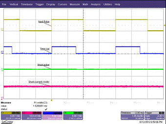
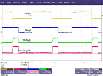
Fig. 4. Cell voltage lower than average. Fig.5. Cell voltage greater than average.
1. Perforated quick proto boards like the one shown on fig. 3 photo are only good to prototyping and checking out logic operation near static (DC) or low frequency circuits, analog or digital. If you're trying to prototype anything running at around 100 kHz or higher, these boards will give you more headache than help. Do not use them to prototype high frequency circuits!
Simple analog BMS for tinkering man – part II
By Victor Tikhonov
President/CTO
Metric Mind Corporation
Published Nov. 11 2012.
This article is the second part of analog BMS description. The first part was published in the December 2012 issue CE. I want to reiterate that this system is not a substitute for sophisticated software-based management systems, nor it meant for those who never held a soldering iron in their hands and don’t like tinkering with electronics. It represents proven, working idea which can be implemented for your particular circumstances. Another reason I describe in detail how it works is so that anyone can take it further, modify it to suit your particular needs. Now it’s good place to insert standard DISCLAIMER:
Even before completing this portion of the article I had several inquiries if I plan to make this system available for purchase for private use. Presently I have no such plans, but that may change. In the past, Metric Mind Corporation allowed DIY amateurs to work on their conversions using the same electronic components supplied to OEMs. However, after several misapplications of expensive hardware by ignorant users coupled with subsequent demands for warranty support etc., I decided to restrict my attention to dealing with professional OEM engineers. If MMC were to produce MIMIC based-BMS, screening and qualifying individuals will be needed. Therefore, for now readers of CE are welcome to use the idea described herein - at your own risk. For the time being, the system described here is not available from MMC - either fully assembled and tested or as a kit. But the understanding the idea behind its operation idea and having electrical schematic to start from is all needed for a skilled person to successfully implement (and improve) this design idea.
THE TRANSMITTER.
The block diagram of the transmitter circuit complementing the MIMIC nodes forms a fully functional system. The transmitter conveys the ‘ideal average’ cell voltage of the traction pack to every MIMIC cell node, for comparison purposes. The block diagram of entire circuit is pretty straight forward and presented on fig. 6 below. It consists of 4 functional blocks: input isolation and scaling, beat pulse generator, voltage to time (V2T) converter and optocoupler’s LEDs driver.
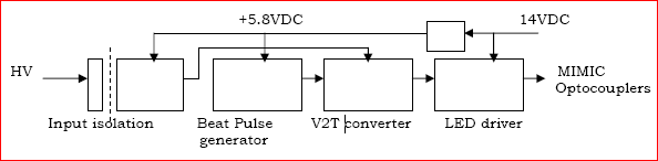
Fig. 6.
HOW IT WORKS
By taking each block individually understanding the whole operation will become self-evident. The first functional block is there to provide two functions: galvanic isolation of the HV (high voltage) input from the rest of the circuit which is referenced to the ground (vehicle chassis) and scale the battery voltage so that block's output represents average cell voltage. Of course, the transfer function from input to output must be as linear as possible. However, while the optocouplers used here are not high-linearity type, the feed back technique used here removes non-linearities of the optocouplers themselves from the equation, and the resulting measurement is more than adequate for practical application like this.
Electrical schematic of the transmitter is presented on fig. 7.
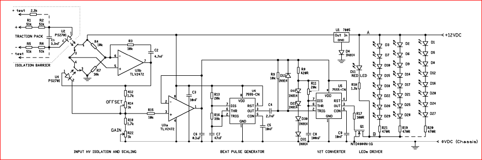
Fig. 7 . Transmitter module
The HV isolator consists of the op amp U3b and the bridge formed by generic optocouplers U2 and U4 in one branch and resistors R4 and R7 in the other. U2 is placed in the measured voltage loop while U4 is in the DC feedback loop. The voltage on inverting input of the op amp is equal to ½ of the supply voltage (R4=R7) or 6 VDC. An op amp output will swing higher or lower to maintain the same voltage on its non-inverting input (that’s basic op amp operation, in this circuit it is called a negative feedback servo-system). That means to balance, the bridge resistance of phototransistor in U4 has to be the same as that of U2 to also divide the full applied supply voltages equally. In this circuit, if the light intensity of respective LEDs in U2 and U4 is the same, that means current flowing through them is the same. The current through U2’s LED is determined by (and is directly proportional to) the traction pack voltage. So, with more voltage – more current – less resistance of U2’s phototransistor – higher voltage on the non-inverting input of the U3b. U3b will compensate this by raising its output so that the current flowing out and through U4’s LED, R18 and R22 becomes equal to U2’s current, (balance) in order for U4’s phototransistor to conduct precisely to the same degree. This brings the non-inverting input voltage back to ½ of supply voltage. This servo loop will track input current essentially mirroring it through the feedback loop. Because output current flows through R18+R22, that voltage drop directly represents U2's current e.g. HV pack voltage.
It is important to note that we can change the value of R22 but the current will stay the same (as it still has to match U2’s current), so the output voltage (voltage drop on R18+R22) will be higher or lower for given current. In other words, we can adjust the gain of the circuit. Ideally, if input voltage is the same as output, in order to maintain the same currents through LEDs R1+R2+R5+R6 should be equal to R18, plus R22. The op amp output voltage must be about 3.2V to represent average cell voltage. However, as we have a very high voltage input, nearly 320VDC or 100 times of the output, we just have to make R1+R2+R5+R6 100 times of the value of R18+R22 in order to maintain the same currents. Users should adjust the circuit by changing total input resistance accordingly for their pack voltage. The R12 and R14 are there to pre-bias non-inverting input of U3A, thereby removing an initial ~1.1V “dead zone” output offset on U3b which is a consequence of the ~1.1V LED drop before it starts conducting current. It works because R12 and R14 start conducting current right away, unlike U4’s LED which has to wait until voltage rises above its threshold of about 1.1V. In this respect R12 and R14 are optional as one would never expect output voltage drop on them to fall below 1.1V - that would represent a very dead cell. With using R12 and R14 you will have permanent output offset of -1.1V, but this is still workable solution.
The rest of the circuit is just a booster stage U3a isolating the high impedance voltage source sampled across R18+R22 from the rest of the circuit. The output of U3a following average cell voltage directly supplies the V2T converter which is almost identical to that of every MIMIC module: it generates pulses whose length is proportional to the average cell’s voltage. Beat pulse generator triggers the V2T converter every 3.3ms (generated repetition rate is 300 Hz) using its falling edge.
Because the V2T directly driven by U3a output, it produces pulses just like MIMIC module does: the duration of each is 2ms for the 3.2V Vdd supply. Since there is no need for a comparator to generate shunting pulse, there is no diode “AND” stage. Instead, output of the V2T directly drives the power FET which connects strings of LEDs to the +12V source supplied by the vehicle’s low voltage accessory 12V net. On the schematic the series strings of LEDs (8 in per string) are actually the LEDs inside of the optocouplers on each MIMIC module. So 3 wire cable is needed as a bus between MIMICs to create this interconnection arrangement – See fig. 8.
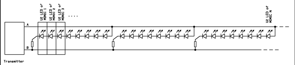
Fig. 8. Each LED is actually an optocoupler of a MIMIC module.
Because of the string of 8 series LEDs , if the number of cells to be monitored is not an even multiple of 8, the series resistor value will need to be increased to maintain the same current (~15mA) through any shorter chain of LEDs. The simple design calculation dictates adding to the base value of 470 ohms already there approximately (1.15V/0.015mA) = 77 Ohm per every absent LED. For instance the last chain of, say, 4 LEDs will have current limiting resistor 470+77*4=778 Ohm. Pick the nearest standard value, i.e. 750 ohm.
COMMENT REGARDING POWER SUPPLY
– For simplicity’s sake and keeping to a low cost the circuit uses a very common LM7805 voltage regulator “padded” by diode D4 to produce an output of about 0.7V higher than rating of a bare regulator. Because the maximum output voltage of the isolator can only be Vdd-Vsat-1.1V (where Vsat is saturation voltage of output stage of the op amp preventing true rail Vdd output, typically 0.25V, and 1.1V is the forward voltage drop on U4 LED), that pencils out it to be 5V-0.25V-1.1V= 3.65V in case of 5V supply, which is very close to the max voltage of fully charged cell. So to give op amp more headroom diode D4 raises Vdd by 0.7V which provides plenty of margin. Alternatively you can just use 7806 or 7809 regulators, but these are not as common as 7805.
For the op amp you can use any part that allows single power supply operation and with sufficient output current to function as power source for everything else. I just had TL2472 op amps on hand, but there are many other suitable parts. Depending on the op amp and whether it has internal compensation you might need to fine tune R3C2 feedback network to ensure there is stable operation and no parasitic oscillations.
As a practical tip: while bundle the wiring together looks clean and neat, keep in mind that long runs of parallel conductors make up pretty good capacitors. So despite the operating frequency being low, you don’t want to skew (shift) pulse edges and introduce delays due to a large capacitance of the bus. So strive to minimize the total length of wiring. A star connection using a few strings directly from the transmitter is preferred, rather than having all MIMICs in one long series connection run. The connection order of MIMICs is not important, as all LEDs carry identical signal, and do not have to follow the path of electrical connection between cells themselves. But a predictable pattern makes for easier troubleshooting later on. Remember to document what goes where. “An ounce of prevention is well worth a pound of cure”
A final note: while it may be tempting to use dual CMOS timer package instead of two separate parts for U5 and U6, beware! This won’t work since the two Vdd supplies for these chips are separated in this schematic but they would be connected together inside dual timer chip. That would become a problem.
TUNING THE CIRCUIT
This is simple – first remove the U3b output offset by adjusting the R14 trimming pot. In my prototype this happened when total resistance of R12+active portion of R14 was 2.26k ohms. The simplest way is to set the wiper at about the half-way mark initially (at 500 Ohm). Then adjust the gain so that input voltage increment causes the same *percentage* output voltage increment. It is easier to accomplish this is before installation in the EV (e.g. on the bench). Apply a precise 3.2V input voltage – the output should follow the input one for one. For this to work, connect a variable power supply directly to “+ test” and “– test” inputs (connection shown with dashed lines, this will bypass R1 R2 R5 and R6. Also use a 2.3k resistor instead.) Now set input voltage to 3.0VDC. Adjust gain pot such that the output of U3a reads a corresponding 3.0V. Next, increase test supply voltage to 3.5V and watch for the incrementing of the U3a output – it should rise to 3.5V as well. If it is less, increase the gain by turning up R22 (do the opposite if output rises to more than 3.5VDC) until 0.5V input increment causes 0.5V output increment – this will happen when actual input and output voltages do not match. Finally, adjust offset trim pot R14 to make actual voltage match. Since the combination of R14+R12 is connected in parallel to U4’s LED, adjusting R14 will shunt this LED to a different degree, which causes the U3b output current to split in two paths (through LED and R12+R14 in different proportions. (This, in turn, means you have essentially changed U4’s Current Transfer Ratio (CTR) and will slightly affect the gain adjustment you just tuned. So in a couple of iterations adjusting R22 and R14 you will achieve the condition where U3a output follows test input precisely. At this time output of U5 will generate pulses about 2ms long.
Now you can disconnect your temporary power supply from +test and -test inputs and connect real high voltage traction battery to the + and – inputs marked on schematic "TRACTION PACK". Pay attention - the "test" inputs are for 3.2V input voltage ONLY! If you accidentally connect high voltage pack to "test” inputs, the current through U2 be is restricted only by low value 2.3k resistor and U2 will instantly blow up! To avoid potential troubles, after initial tuning the circuit on the bench with 3.2V supply on "test" inputs it's better to physically remove 2.3k resistor (in series with +test lead) from the PCB.
Now the system is ready for commissioning. Total resistance of R1+R2+R5+R6 should be about as many times larger than the sum of R18+active portion of R22, as many cells you have in your pack. The total input resistance affects gain the same way as R22 does. Note the power dissipated on R1, R2, R5 and R6 - make sure their power rating is adequate. (that's another reason 4 resistors are used instead of one - each will have to handle only 1/4 of the power of one)
When everything is in place and functions, you would want to make sure the “turn-on threshold” of each mimic is the same (set with by R4 – refer back to part 1 of the article). While turning R22 from limit to limit, you will change output of U3a by at least +/- 0.5V, making the ‘average cell’ value artificially 0.5V lower or higher than it really is. This in turn will cause all or none MIMICs to shunt their cells, which is a good way to verify if you have any abnormally high or too low voltage cells. You’d want to set R22 just under threshold so that the ‘average cell’ is slightly larger voltage than real cells, so none is normally shunted. As soon as any cell exceeds this average, it will gradually increase the time its FET is on and shunts the cell – this can be observed by watching D2 LED on each MIMIC module.
IMPROVING THIS SYSTEM
You may notice that the maximum shunting duty cycle can never be much more than 50%, and this value decreases when it’s needed most – near the end of a recharge. This is because the timer must “expend” first 2ms of the total 3.3ms cycle to sample input voltage, since the information about the average cell value is contained within this 2ms time slot. The circuit cannot start shunting until it understand if it is really 2ms or not, and if you start shunting right away after trailing edge of the "information pulse", you have only 3.3-2.0 or1.3ms (out of the slot of 3.3ms) to do it. What can be done is to add a second timer to the MIMIC module (using a dual 555 CMOS timer chip) in a monostable fashion (t=~3.3ms), triggering it by the output of the first one. This way for as long as the cell voltage exceeds average cell voltage, the shunt turns on hard and shunting duty cycle is 100%, providing more aggressive control. What is lost is the fine proportional degree of shunting, but the action will happen faster. In general – if using good quality, closely match cells, the original method described above will yield better results. If your cells are mismatched, more crude and brutal on/off control may more effectively keep them from overcharging, but remember – any BMS is not there to fix bad cells! It is there to compensate for inevitable *normal* variations in SOC due to manufacturing tolerances and different environmental conditions (such as front and back partial pack enclosures' temperatures) for each cell causing that gradual SOC divergence - there is simply no mechanism to inherently equalize cells as the pack ages and is repeatedly cycled. In a series string each cell doesn’t know about existence of other cells (other than sometimes sensing heat of adjacent cells).
COOLING
Make sure there is adequate cooling for all shunt resistors. Do not buy 5W rated shunt resistors if you want to dissipate 5 watts (shunt current is 1.5A which means power dissipation is at cell voltage of 3.2V is 3.2V*1.5A=~5W). Resistor will not glow red but will be hot enough to unsolder itself from the PCB and the circuit will fail in a hurry. Study the data sheet for those power resistors carefully to see the temp raise rating vs. dissipating power. It might be tempting to choose low resistance shunts to tame misbehaving cells, but remember, using 100 individual shunts that are all on at once will produce ~0.5kW of waste heat for this example! That’s nearly as bad (and hot) as having ten regular 50W incandescent light bulbs on at the same time inside [normally] enclosed box. Aside being wasteful, give thought as to how best to get rid of all this heat! It is common for application circuits to omit such components as bypassing capacitors or safety fuses, commonly accepted as default. More-less experienced circuit designers will know this. Such components serve a purpose, so don’t forget them. Bypassing the incoming 12V supply with 1,000uF electrolytic cap (watch its low temp. ratings!) will be sufficient. Consider adding reverse polarity protection by using a forward biased diode in series +12V supply rail. If you have any questions about described system, always welcome to drop me a line to tech.support@metricmind.com.
Happy EV'ing,
Victor Tikhonov
MMC
November 2012